Semiconductor Field · Category Overview
Compound semiconductor manufacturing — silicon carbide (SiC), gallium arsenide (GaAs) and gallium nitride (GaN) — runs on hot zones that cannot tolerate metallic contamination or thermal drift. Dehong's semiconductor-field lineup insulates and supports those hot zones end to end, from source-material synthesis through crystal growth and downstream epitaxial processing.
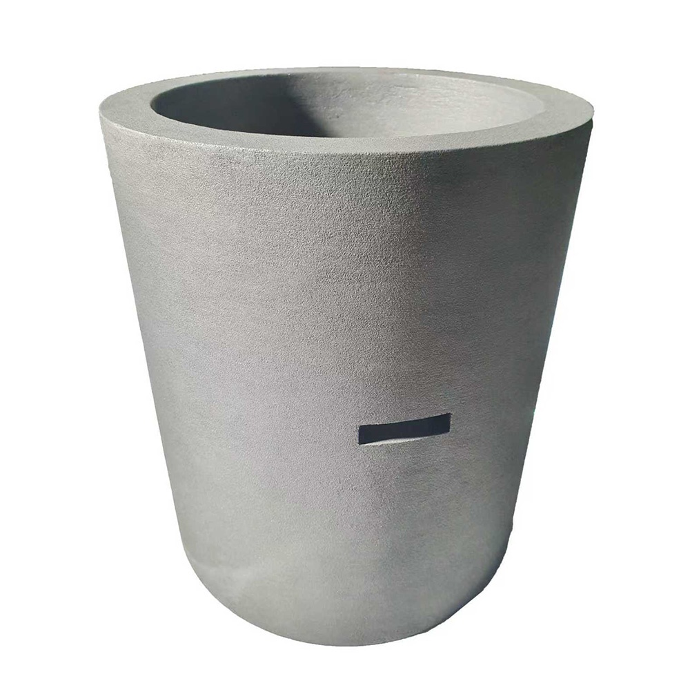
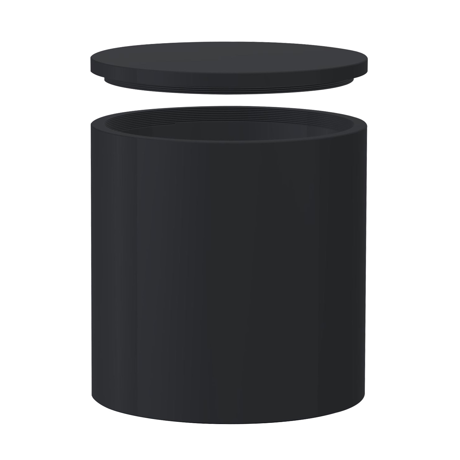
Graphite crucibles hold source powder through the reaction that fixes stoichiometry before crystal growth begins, resisting aggressive vapor-phase chemistry at temperature.
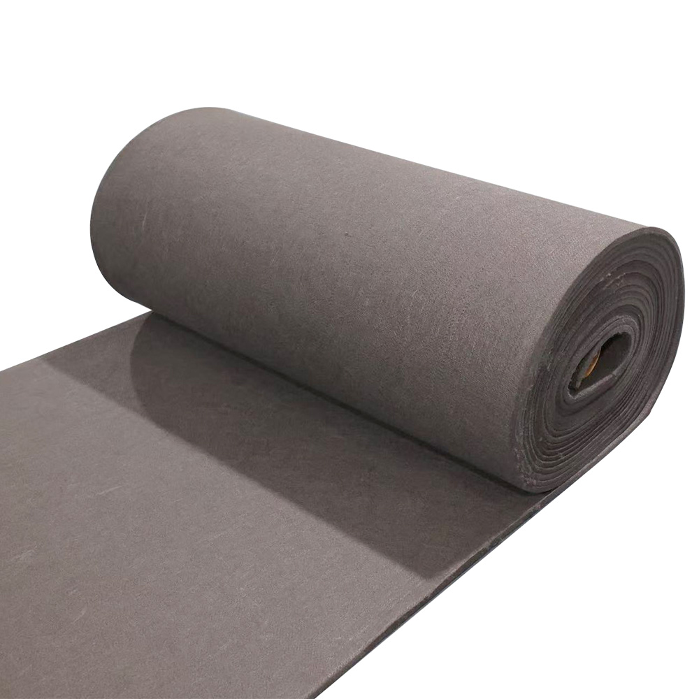
Soft insulation felt and viscose-based hard felt tubes hold the axial thermal gradient that governs crystal polytype, cutting heat loss without shedding particulates into the chamber.
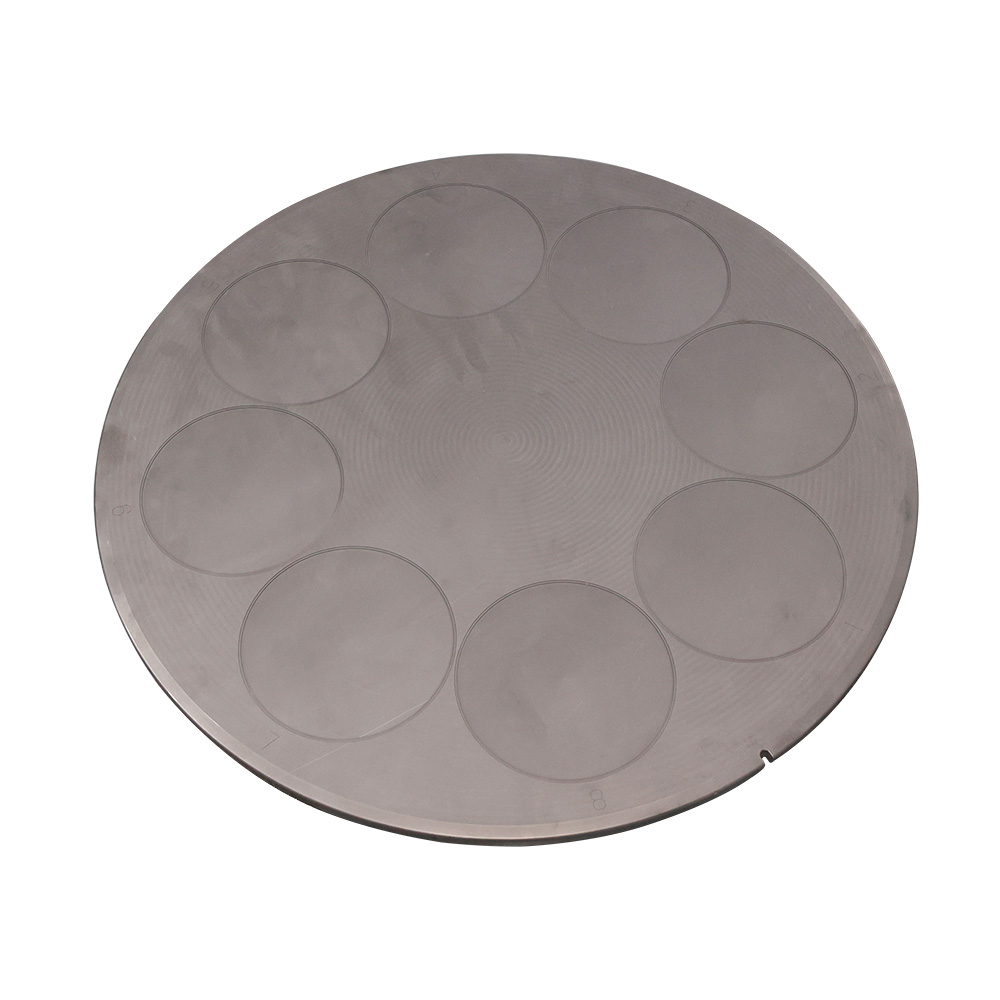
Graphite epitaxial wafers act as susceptors for downstream deposition, providing an even, low-impurity platform for growing device-grade semiconducting layers.
Ash content and metallic-impurity levels are held to semiconductor-grade purity, protecting melt and vapor-phase purity where even trace metals can shift device yield.
Fiber architecture in the felt and crucible bodies arrests crack growth, so hot-zone geometry and insulation performance hold steady across thousands of heating cycles rather than degrading run to run.
Engineering Heritage
The felt, felt tubes, crucibles and epitaxial wafers used in the synthesis and crystal-growth stages draw on the same fiber-and-matrix engineering Dehong applies across its solar PV, battery, vacuum-furnace and preform product lines — carried through preform design, densification and graphitization rather than sourced as generic graphite parts.
Fiber architecture, density grade and densification cycle are matched to each semiconductor-field component's load and purity requirement, not applied as a one-size fit.
Preform fabrication, CVI/LPI densification, graphitization and machining are run in-house, so purity and dimensional control carry through from raw fiber to finished felt tube or crucible.
Development is backed by an ISO 9001 quality management system, a Municipal-Level Enterprise Technology Center, a Provincial R&D Center, and over 30 filed patents covering C/C process and component design.
Manufacturing
Each batch of soft felt, hard felt tube, graphite crucible and epitaxial wafer moves through the same controlled sequence, with purity and dimensional checks confirmed before shipment.
Frequently Asked Questions
Soft insulation felt is flexible and lightweight, suited to wrapping irregular hot-zone surfaces where easy handling and installation matter. Viscose-based hard felt tubes are rigid, higher-strength components used where the insulation also needs to hold its own shape and resist mechanical load over long duty cycles.
Trace metallic impurities from crucibles or felt can diffuse into the melt or vapor phase during synthesis and crystal growth, altering dopant behavior and reducing device yield downstream — which is why compound-semiconductor processes specify high-purity graphite and C/C over standard industrial grades.
Service life depends on operating temperature, atmosphere and cycle frequency, but well-densified C/C and high-purity graphite components are engineered to resist thermal shock across thousands of heating cycles before mechanical or purity performance declines.
Yes. Fiber architecture, density grade, felt thickness, crucible bore dimensions and purity grade can all be matched to a customer's furnace drawings, OEM part numbers or process targets, with a matched material spec confirmed before production tooling begins.
Wafers and crucibles should be inspected for surface contamination and handled only with clean, non-abrasive tools to protect purity. Crucibles should also be preheated gradually before use, since sudden temperature changes can crack or prematurely wear an otherwise sound component.